
Silicon Carbide Photomasks Market to Reach USD 521.3 Million by 2034 as Precision Pattern Transfer Demand Expands
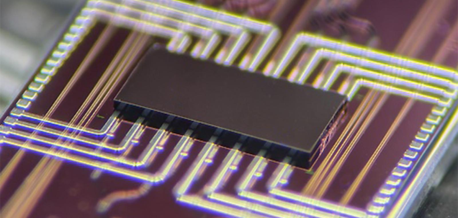
Semiconductor manufacturing requires precise pattern transfer as device architectures become more complex and process qualification standards evolve. Photomasks act as image-transfer masters in lithography, while coating composition, optical response and defect control influence their performance in semiconductor production.
According to SemiconductorInsight, the Global Silicon Carbide Photomasks Market was valued at USD 280.4 million in 2025 and is expected to reach USD 521.3 million by 2034, growing at a CAGR of 7.1% over the 2026–2034 forecast period. Revenue for 2026 is estimated at USD 300.4 million as mask shops, foundries and power-device manufacturers expand precision pattern-transfer capacity.
Explore the complete Silicon Carbide Photomasks Market analysis: https://semiconductorinsight.com/report/silicon-carbide-photomasks-market/
Why Are Silicon Carbide Photomasks Important in Semiconductor Manufacturing?
Photomasks serve as image-transfer masters in semiconductor lithography. Optical projection systems use their patterns to transfer circuit designs onto photoresist layers on semiconductor wafers.
Mask performance depends on absorber-film uniformity, line-edge quality, exposure wavelength, defect levels and repair history. Coating layers can also influence optical response, surface durability and process compatibility.
The report covers patterned photomasks and related qualified mask layers where silicon-carbide-related functional constituents are specified within the market scope. It does not include lithography scanners, all SiC wafers or complete mask-writing equipment systems.
Customers must validate the coating stack, optical characteristics, defect mapping and cleaning stability before qualifying a mask for a specific manufacturing process.
Market Growth Is Closely Linked to Semiconductor Patterning Requirements
The demand for qualified photomasks is influenced by semiconductor manufacturing activity and the need to transfer increasingly complex device patterns. Foundries and mask shops require products that meet process-specific optical and dimensional specifications.
Semiconductor Insight identifies Asia-Pacific as the largest regional market, with an estimated 51% share. Japan, Taiwan, South Korea and China combine mask manufacturing capabilities with dense semiconductor production networks.
As power-device manufacturers introduce new trench, junction-termination and contact architectures, mask layers must be qualified for the intended process and exposure conditions.
The market should be distinguished from broader lithography equipment spending and the value of semiconductor wafers or finished chips.
Receive your Free Sample Report today: https://semiconductorinsight.com/download-sample-report/?product_id=139401
Transmission Rate Categories Shape Product Segmentation
The report segments the market by transmission rate, with 90% transmission products representing an estimated 44% share. The 85% category accounts for approximately 27%, while 80% transmission products represent around 19%. Other variants account for approximately 10%.
These transmission categories describe market-defined optical product variants and should not be treated as universal limits across all exposure wavelengths or reflective EUV architectures.
Mask selection depends on the full optical system, coating recipe, inspection conditions and pattern complexity. Customers must verify optical response and process compatibility before adopting a particular mask configuration.
Coating Functions and Technology Nodes Create Additional Demand
The market includes functional coating categories such as anti-reflective coatings, hard-mask layers, protective films and other structures. These functions can influence optical response, surface durability and process compatibility.
The report also segments demand by technology node, including above-28 nm, 7–28 nm and below-7 nm categories. These groups reflect different patterning and qualification requirements across semiconductor manufacturing.
Foundries and integrated device manufacturers evaluate coating composition, optical properties, defect levels and cleaning stability when qualifying masks for production.
The report identifies semiconductor chip manufacturing as the largest application category, with lithography-related development and other applications also contributing to demand.
Advanced Mask Materials and Process Qualification Are Key Trends
Photomask manufacturers and semiconductor customers continue to evaluate coating materials and functional layers that can support durability, optical performance and process stability.
The supply chain includes finished-mask manufacturers, mask-blank suppliers, material providers and advanced fabrication centers. These companies occupy different positions and should not be treated as equivalent suppliers of completed photomasks.
Tekscend Photomask, formerly Toppan Photomasks, operates in the merchant-mask market. Shin-Etsu supplies quartz and absorber-layer blanks, while Advanced Mask Technology Center is involved in specialized mask fabrication.
EUV reflective reticles use a different optical architecture from conventional transmissive masks. Transmission-rate categories should therefore not be applied indiscriminately to all photomask technologies.
Defect Control and Material Qualification Remain Key Challenges
Photomasks must maintain pattern fidelity and low defect levels because mask defects can affect wafer imaging and downstream device quality. Customers evaluate absorber uniformity, line-edge quality, optical response and inspection results.
Functional films and coating stacks require validation for cleaning stability, durability and compatibility with the intended exposure wavelength. A mask cannot be assumed interchangeable with established quartz-chrome or molybdenum-silicon architectures without process qualification.
The production chain requires writing, etching, cleaning, inspection, repair and final certification. Capacity is constrained by the slowest qualified tool or review stage.
High equipment costs, strict defect tolerances and customer-specific qualification can delay the introduction of new mask products into production.
Access the Full Report for In-Depth Insights: https://semiconductorinsight.com/report/silicon-carbide-photomasks-market/
Where Are the Biggest Opportunities Emerging?
The expansion of power-device manufacturing creates opportunities for photomask suppliers supporting new SiC device architectures and precision pattern-transfer processes.
Anti-reflective coatings and hard-mask layers represent important functional-film categories. Suppliers able to document coating composition, optical response and defect performance can address specialized customer requirements.
Advanced mask fabrication and regional semiconductor investment provide opportunities for companies developing differentiated coating technologies and qualified mask products.
Foundries and integrated device manufacturers remain important customer groups because they specify and procure masks for semiconductor production and process development.
Future mask formats and lithography architectures may create new technical requirements, although emerging initiatives should not be treated as confirmed demand for the market’s existing transmission-rate categories.
Supplier Qualification and Optical Performance Influence Competition
Photomask suppliers compete through pattern accuracy, defect inspection, coating consistency, optical response, durability and customer qualification support. These factors influence repeat orders and the ability to serve semiconductor manufacturing processes.
The competitive ecosystem includes mask manufacturers, quartz and coating-material suppliers, lithography equipment companies and specialist fabrication businesses. Their roles differ across the value chain.
Semiconductor Insight identifies Tekscend Photomask, Photronics, Dai Nippon Printing, Shin-Etsu Chemical, HOYA, AGC, FST Corporation, Taiwan Mask Corporation, Shenzhen Qingyi Photomask, AMTC, ASML Holding, SK Siltron, LG Innotek, Compugraphics and Advanced Reproductions Corporation among the companies profiled.
ASML supplies lithography systems rather than representing all completed mask sales, while blank and material suppliers support downstream mask fabrication.
Competition is shaped by the ability to meet process-specific requirements and maintain consistent performance across successive mask orders.
Silicon Carbide Photomasks Market Segmentation
The report evaluates the market by transmission rate, coating function, technology node, application and region, providing a detailed view of photomask demand.
By type, the market is divided into:
· 90% Transmission Rate
· 85% Transmission Rate
· 80% Transmission Rate
· Other Transmission Variants
By application, the market covers:
· Semiconductor Chip Manufacturing
· Lithography Development and Qualification
· Other Applications
Additional segmentation covers anti-reflective coatings, hard-mask layers, protective films and other coating functions, alongside above-28 nm, 7–28 nm and below-7 nm technology-node categories.
View the complete Silicon Carbide Photomasks Market segmentation and forecast: https://semiconductorinsight.com/report/silicon-carbide-photomasks-market/
Regional Silicon Carbide Photomasks Market Outlook
Asia-Pacific represents the largest regional market with an estimated 51% share, supported by mask manufacturing and semiconductor production networks across Japan, Taiwan, South Korea and China.
North America accounts for approximately 24% of the market, supported by established semiconductor ecosystems, mask suppliers and customers requiring specialized coating and patterning capabilities.
Europe represents around 19% of the market, with advanced mask suppliers and semiconductor manufacturing activity contributing to demand. The region also includes specialized mask-fabrication and development operations.
Other regions account for the remaining share and often depend on imported precision mask blanks, finished masks or external pattern-writing services. Regional demand is influenced by the location of mask fabrication and semiconductor manufacturing operations.
Competitive Landscape and Key Companies
The Silicon Carbide Photomasks Market includes global photomask manufacturers, material suppliers and companies involved in advanced lithography systems and specialized mask fabrication. Competition is influenced by coating technology, defect control, optical performance and customer qualification.
Semiconductor Insight identifies Tekscend Photomask (formerly Toppan Photomasks), Photronics, Dai Nippon Printing, Shin-Etsu Chemical, HOYA Corporation, AGC, FST Corporation, Taiwan Mask Corporation, Shenzhen Qingyi Photomask, Advanced Mask Technology Center, ASML Holding, SK Siltron, LG Innotek, Compugraphics and Advanced Reproductions Corporation among the companies profiled.
The roles of these companies differ across the supply chain. Merchant mask manufacturers produce finished photomasks, material suppliers provide blanks and films, and ASML supplies lithography systems rather than directly representing all completed mask sales.
What Does the Silicon Carbide Photomasks Market Report Cover?
The Semiconductor Insight study provides analysis of market size, sales, revenue, competitive positioning, industry dynamics, segmentation and regional performance for silicon carbide photomasks and related qualified mask layers.
The report examines transmission-rate categories, coating functions, technology nodes and applications. It also evaluates market drivers, restraints, challenges, process qualification requirements and competitive developments across the mask supply chain.
Regional coverage includes Asia-Pacific, North America, Europe and other markets, with analysis of semiconductor manufacturing activity and the supplier networks supporting photomask production.
Key Questions Answered by the Study
The report helps industry participants evaluate questions including:
· What is the current Silicon Carbide Photomasks Market size?
· How large will the market become by 2034?
· What is the expected CAGR during the 2026–2034 forecast period?
· Which transmission-rate category accounts for the largest share?
· What are the major coating functions covered in the report?
· How does technology-node demand influence photomask requirements?
· Which applications account for the largest market share?
· Which end users represent important customers for photomasks?
· Why is defect control important in photomask manufacturing?
· Which regions represent important markets?
· Who are the leading companies profiled in the market?
· How do material suppliers and finished-mask manufacturers differ?
Explore the full Silicon Carbide Photomasks Market forecast and competitive analysis: https://semiconductorinsight.com/report/silicon-carbide-photomasks-market/
Get a Sample Report copy for free: https://semiconductorinsight.com/download-sample-report/?product_id=139401
About Semiconductor Insight
Semiconductor Insight provides market intelligence and industry research covering semiconductor technologies, electronic components, advanced manufacturing systems and related technology markets. Its research focuses on market sizing, forecasting, competitive landscapes, technology trends, segmentation and regional analysis to support strategic decision-making across the semiconductor ecosystem.
Contact Semiconductor Insight
Website: www.semiconductorinsight.com

 English
 Arabic
 French
 Spanish
 Portuguese
 Deutsch
 Turkish
 Dutch
 Italiano
 Russian
 Portuguese (Brazil)
 Greek